Pcbcart will provide you with high quality pcb fabrication and flexible pcb assembly services that meet your unique requirements.
Blind and buried vias fabrication.
And that is also why they are called buried vias.
Blind and buried vias.
Custom blind and buried vias fabrication from professional and experienced pcb board supplier at low cost.
Adding blind or buried vias can tackle high density and eliminate layers.
Thus they never join the outer layers i e the bottom or top layer of pcb.
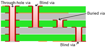
Blind vias start on an outer layer but terminate on an inner layer.
Blind buried vias via in pad tolerances electrical test.
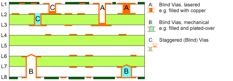
A blind or buried via can be processed in a wide range of different measures including plugged copper mask via a plugged solder mask via plated via or staggered via.
A blind via connects exactly one outer layer with one or more inner layers.
If you re not familiar with these types of vias here s how they can save on fabrication cost.
Let s use the example of an 8 layer design with a 300 pin bga.
Assembly equipments smt packages package on package box build assembly free dfm check.
However the distinct difference between buried and blind vias is that buried via only connects the inner layers.
Use a core thickness as much as possible.
For this reason we often use a blind via or buried via instead.
In general the difference is that a pcb blind via connects the outermost layer to one or more inner layers but doesn t go through your whole pcb.
You cannot see them from the outside.
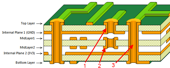
Blind vias and buried vias are not mutually exclusive and a design can employ either or both.
First we start with traditional multi layer boards.
The inner layer try to use same type copper thickness and same copper thickness at both sides of each core.
A buried via is a via between at least two inner layers which is not visible from the outer layers.
The structure of a standard multi layer circuit board is a process including an inner layer line and an outer layer line followed by drilling and metallization in the hole to achieve the internal connection function of each layer line.
Fabrication suggestion of blind and buried vias the best is a symmetrical structure to prevent the expansion caused by inconsistent pcb in serious warpage.
Blind and buried vias help to save pcb real estate by allowing features and lines to be designed above or below them without making a connection.
About half the pins on this bga will be power ground and about half of those will be ground.
Today s high density pcbs frequently require at least the use of blind vias to increase the yield at the fabricator and the assembler.
10 000 served customers in 80 countries.
Blind and buried vias are two options you have for making connections between layers of a printed circuit board and they re both useful when you need as much real estate as possible.
Blind buried vias due to the increasing complexity of design structures blind vias and buried vias are increasingly used in high density circuit boards hdi pcb.
Buried vias exist only between inner layers and do not begin or terminate on an outer layer.